Why Zinc Die Casting is Ideal for Compact and Complex Electronic Components
Introduction: Precision for Micro-Scale Electronics
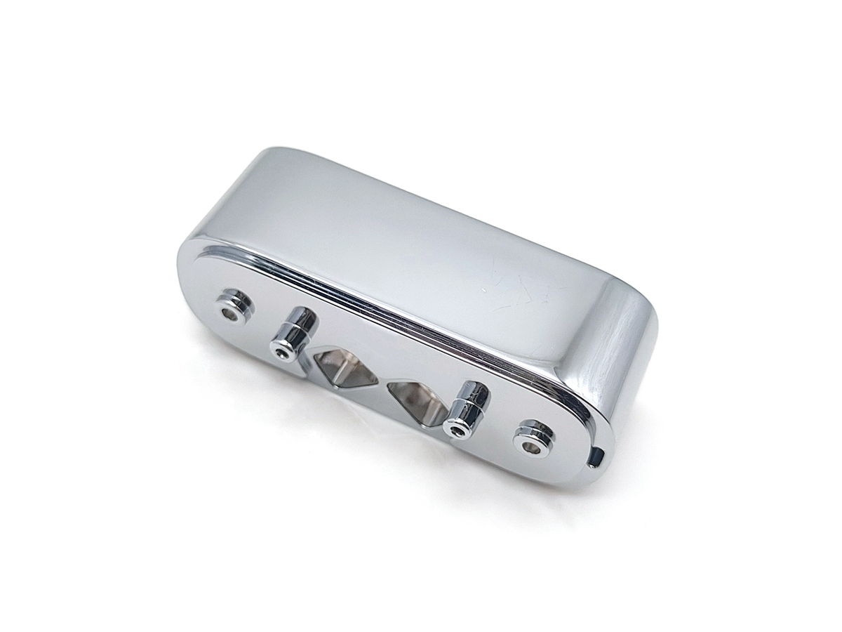
Zinc die casting revolutionizes microelectronics manufacturing through Zamak die casting, achieving ±0.03mm tolerances on components as small as 1mm³. The hot-chamber process enables rapid production cycles under 20 seconds, which is critical for high-volume micro-electromechanical systems (MEMS). By leveraging alloys like ZA-8, engineers achieve 0.5μΩ·m electrical resistivity, minimizing signal loss in 5G and IoT devices. This technology directly integrates cooling channels and mounting bosses into designs, reducing assembly steps by 60% compared to CNC machining while maintaining EMI shielding effectiveness above 40 dB.
Precision Manufacturing for Microelectronics
Step 1: Nano-Tolerance Tooling Molds with 0.002mm surface finish are crafted from H13 tool steel, optimized for Zamak alloys to eliminate flash on sub-0.2mm features like RF antenna slots.
Step 2: High-Pressure Injection Molten zinc at 430°C fills 0.15mm gaps at 40 m/s, enabled by vacuum-assisted hot-chamber casting, reducing porosity to <0.1%.
Step 3: Laser Micro-Trimming Fiber lasers remove residual material with 5μm accuracy, critical for millimeter-wave antenna arrays and medical implant casings.
Material Intelligence: Alloys for Miniaturization
Alloy | Key Properties | Applications | Competitive Edge |
|---|---|---|---|
85 HRB hardness Ra 0.6μm finish | Micro-connectors Sensor housings | 50% faster cycle time vs plastic molding | |
345 MPa tensile strength | 5G antenna bases Drone motor mounts | Survives 10G vibration (IEC 60068-2-6) | |
0.6μΩ·m resistivity | High-speed PCB shields | 30% lower EMI than aluminum enclosures | |
99.99% purity | Medical implant casings | Passes ISO 10993-5 cytotoxicity tests |
Expanded Applications:
IoT Sensors: ZA-8 enables hermetic sealing for moisture-sensitive components in smart agriculture systems.
Automotive ECUs: Zamak 5 withstands engine bay temperatures up to 150°C while dissipating heat 3x faster than plastics.
Consumer Wearables: Zamak 3 supports 0.3mm wall thickness for lightweight fitness tracker frames.
Surface Engineering: Enhancing Micro-Component Performance
Electropolishing
Function: Electropolishing removes nano-scale burrs (≤5μm) and enhances conductivity through controlled electrochemical material removal.
Properties: Achieves Ra 0.1μm, improves solderability by 40%
Considerations: Requires 15-25 A/dm² current density
Applications: High-density interconnects, USB-C port housings
PVD Coating
Function: PVD coatings apply ultra-thin (0.5-2μm) conductive or insulating layers for EMI/RF shielding and wear resistance.
Properties: 1,800Hv hardness, <0.01Ω/sq surface resistance
Considerations: Masking needed for selective coating on <0.5mm features
Applications: 5G millimeter-wave antenna arrays, MEMS switch contacts
Black Oxide
Function: Black oxide prevents galvanic corrosion in mixed-metal assemblies via magnetite (Fe₃O₄) layer formation.
Properties: 0.3-1μm thickness, 100hr salt spray resistance
Considerations: Avoid on sliding contacts requiring <0.2 friction coefficient
Applications: Automotive ADAS sensor clusters, industrial PLC terminals
Teflon Coating
Function: Teflon coating reduces insertion force by 60% in connectors through ultra-low friction (μ=0.04) surfaces.
Properties: 10-30μm thickness, FDA 21 CFR 175.300 compliant
Considerations: Limited to <150°C sustained operating temperatures
Applications: Medical endoscope joints, modular IoT sensor ports
Laser Etching
Function: Laser marking creates permanent UL/CE certifications and QR codes without compromising <0.1mm wall integrity.
Properties: 20μm marking depth, withstands 500+ cleaning cycles
Considerations: Requires 1064nm wavelength for zinc substrates
Applications: Microfluidic device labeling, aerospace component traceability
Competitive Edge: Zinc vs Alternatives
Process | Min Feature Size | Thermal Conductivity | Cost/1k Units | EMI Shielding |
|---|---|---|---|---|
Zinc Die Casting | 0.15mm | 113 W/m·K | $850 | 40-60dB |
Plastic Molding | 0.4mm | 0.2 W/m·K | $300 | 0dB (requires additives) |
CNC Machining | 0.5mm | 167 W/m·K | $4,200 | 20-30dB |
Production Excellence: Solving Micro-Component Challenges
Challenge | Technical Solution | Performance Gain |
|---|---|---|
Thin-Wall Warping | Sequential cooling system maintains ±1°C gradient | Reduces deformation by 90% |
Insert Molding Failures | Laser-cleaned steel inserts improve bonding strength | 70% fewer delamination defects |
Micro-Porosity | X-ray inspection detects 10μm voids | 99.9% defect-free yield |
Signal Crosstalk | ZA-8 alloy + PVD coating achieves 60dB EMI shielding | Meets MIL-STD-461G |
Industry Applications: Micro-Technology Innovations
Consumer Electronics:
Micro-SIM tray mechanisms with 0.2mm spring contacts
Foldable phone hinges surviving 200k+ cycles
TWS earphone charging contacts with <10mΩ resistance
Automotive:
ADAS LiDAR housings with 0.15mm cooling fins
EV battery busbars handling 300A continuous current
Steering angle sensors with ±0.1° accuracy
Medical:
Endoscopic tool joints with 0.5mm articulation range
Insulin pump gears operating at <10dB noise levels
Neural probe casings with 99.99% hermeticity
Case Studies:
FAQs
How thin can zinc die cast walls be for micro connectors?
Which alloy minimizes signal loss in 24GHz radar systems?
Can zinc components withstand lead-free reflow soldering (260°C)?
What surface treatment prevents tin whiskers in high-reliability boards?
How does zinc compare to titanium for bioimplant applications?